Board Bring Up and Testing
Having worked through the slight pain of the early GTEM board setup, which used the ATM90E26 and required a more time consuming, rigorous test and calibration routine, in designing the subsequent board, it was really important that this could be made much easier. This applies not only from production test point of view, but also the end user.
A positive advantage of the ATM90E32 and ATM90E36, over the ATM90E26 device, is that with a known test setup, the calibration is almost non-existent – it is really only voltage calibration that may need a minor tweak at the users end depending on the transformer used.
The Board Design
It all starts in the R&D, concept, schematic and board design. With a thought out schematic and board layout, where the end manufacturing and test process is considered, equal to the board R&D and functionality importance, with all components being surface mount and resistors of 1% tolerance, or less, confidence in safety and build quality must be consistent.
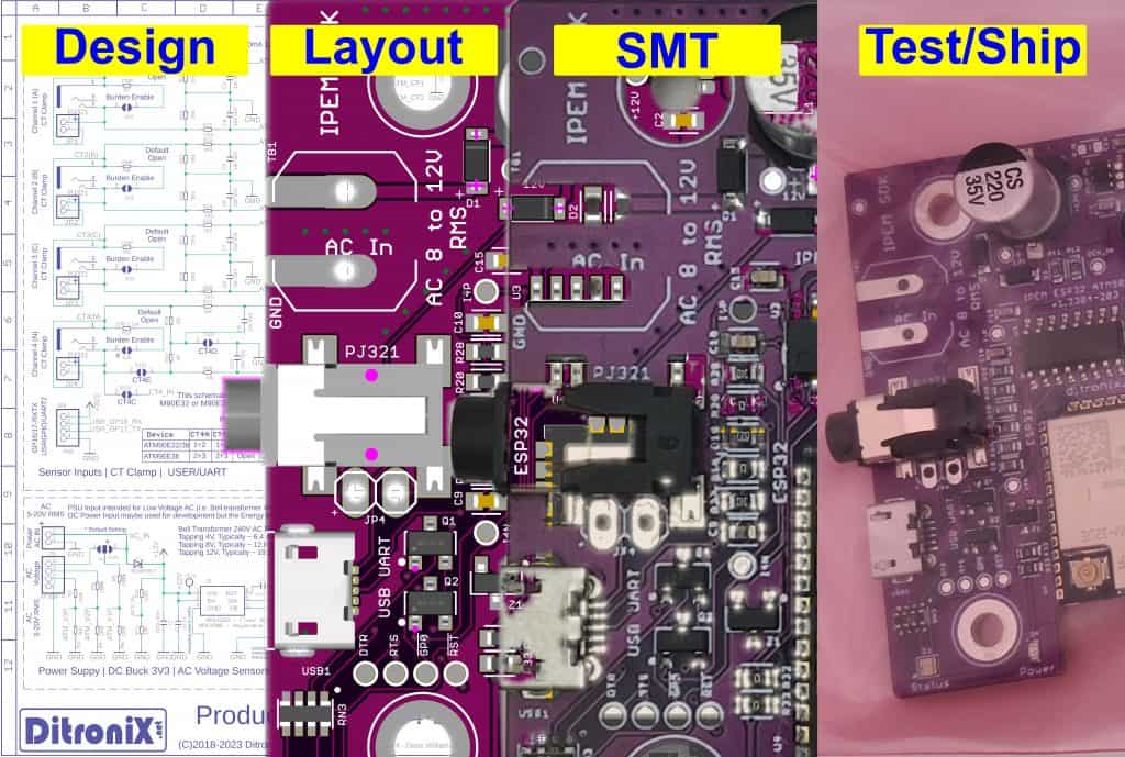
Some of you may realise, I have a version of Engineering OCD and it is really important to me that testing of the all my boards, goes through a strict but straight forward methodical process. It is equally important that I am confident all boards are tested and of a known state, before being packaged and shipped.
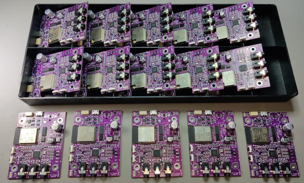
Every IPEM and IPEC board goes through a production bring-up power test and then a calibration and final test. Current production is 100% pass on all counts.
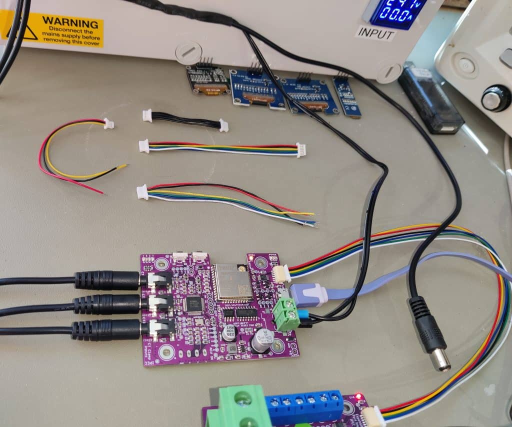
Bring Up Test and Calibration Test
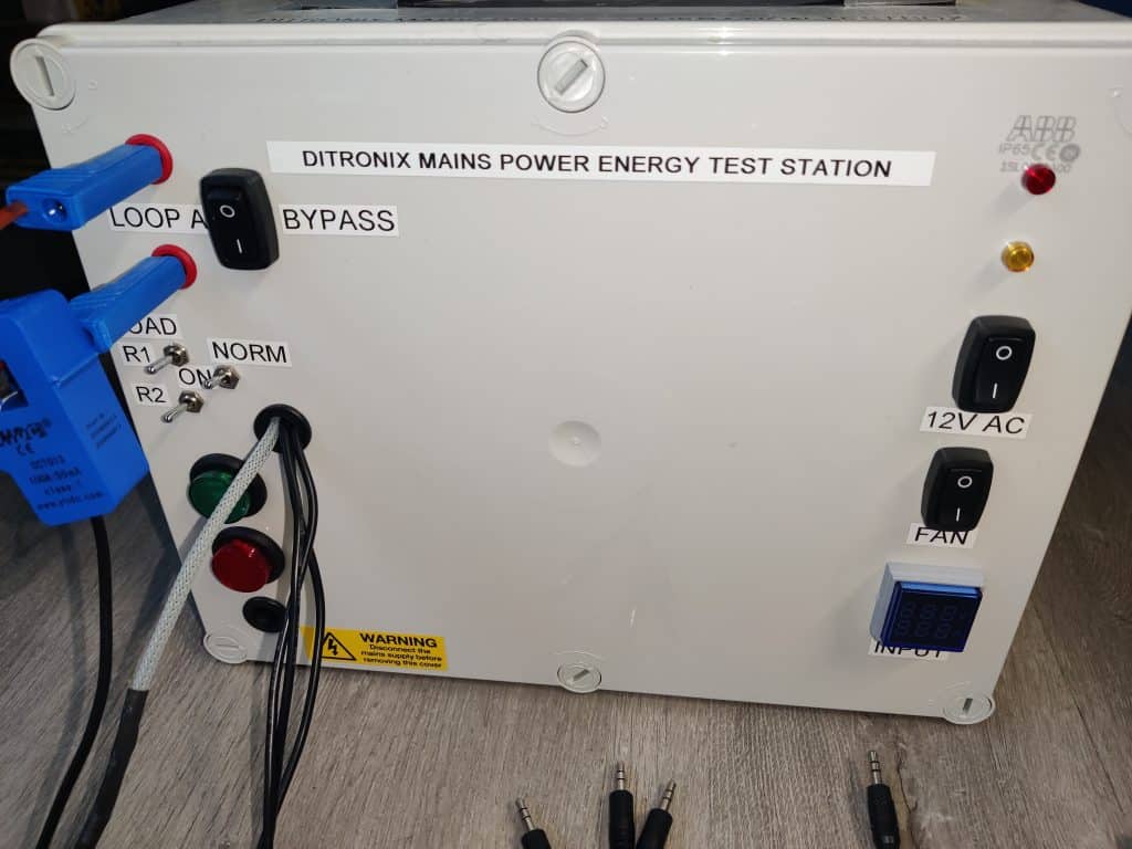
In order to be consistent in testing, save time and importantly do this safely, a Mains Power Calibration TestBox was made.
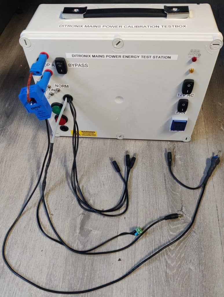
The prerequisite for the test box was:
- Safety
- Consistency and Ease in Testing
- Ability to test single, split and three phases
- Ability to switch Import/export test
- Flexibility in Testing. *Small load, large load etc*
- Time Saving *Without Cutting corners*
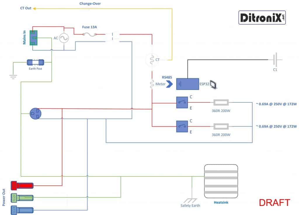
The key components are essentially:
- Three standard YHDC SCT-013-000 (100A/50mA), current clamps. *All going through a single phase live wire, so I can test consistency of the three channel outputs from the same single source.*
- One DAT01A transformer using the 12V tapping. *This produces around 18V RMS AC and powers the test board, plus provides an AC feed for reference.*
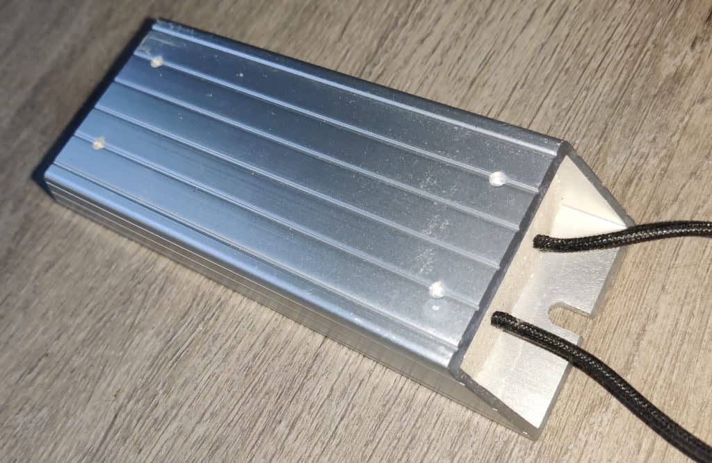
- Switchable resistive loads bolted to an internal heatsink. *Typically these are 200W @ 360 Ohms.*
- Thermostatically controlled heatsink fan
All boards are individually tested and logged, using my homebrew lab calibration box.
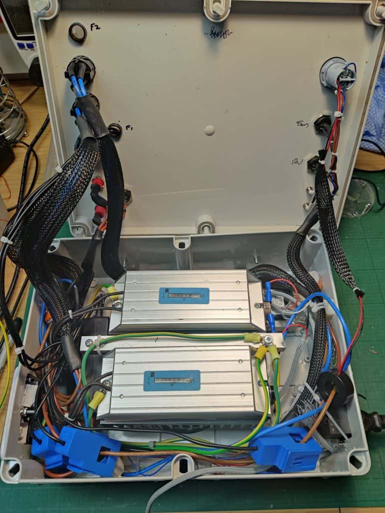
An Internal Photo (During Build)
The boards serial debug outputs are consistent in value readings which is an important milestone.
Test Flashing
Early testing all started with a bunch of various Arduino code. This proved messy and inconsistent in test flow, so with the need to ramp up the various board functionality, and then check calibration for both E32 and E36, the code was merged, ported to Platform IO and massively expanded over time. The IPEM release in GitHub of ‘IPEM_1_Test_Code_ATM90E32_ATM90E36’, is what is used for testing the boards in the lab, as well as used and adapted by users.
As you may have realised, more so if looking through the code, this has really evolved into quite a large application firmware. It certainly now needs a revamp but it works and with this is mind, and with the new IPEC board, coupled with the IPEX, I decided to merge in IPEC/IPEX functionality too. The reason being, it is a single piece of manageable code for ALL Power Energy Monitor boards (except the older GTEM).
Final Test
Now that we have a board which has been flashed with a known build standard, the 12V and current clamps are connected and the firmware debug output is checked.
Test Code Example Output
IPEC Test Firmware Output Example

Configuring Board.. Please Wait..

Hardware Options and Auto Configuration

Scanning I2C Bus for Devices for Auto Configuration ...
I2C Possible Device(s) found at Address:
* Hex 0x40 (64) PCA9685 12bit IPEX PWM Driver
* Hex 0x49 (73) ADS1115 16bit IPEX1 ADC
* Hex 0x50 (80) EEPROM
* Hex 0x60 (96) MCP4728 12bit IPEC DAC
* Hex 0x70 (112) PCA9685 12bit IPEX PWM 'All Call'
I2C Bus Scan Complete

IPEC/IPEX1 ESP32 ATM90E32 MCP4728 ADS1115 PCA9685 IoT Power Energy Monitor Controller

IPEC/IPEX1 Register Status and Startup Report
ESP32 Serial ID: E055F4519140
Firmware Version: 230809
Board Location: House

Preparing New EEPROM. Full Formatting... Please Wait...
|~~~~|~~~~|~~~~|~~~~|~~~~|~~~~|~~~~|~~~~~~~|~~~~|~~~~|~~~~|~~~~|~~~~|~~~~|~~~
EEPROM Cleared and Ready

EEPROM Check: 20 (Validation OK)

DAC MCP4728 Initialised
DAC Output is Enabled from DAC Test Output
DAC Output Voltage Minimum V: 0.000
DAC Output Voltage Maximum V: 3.300
DAC Minimum Power Threshold W: 0005
DAC Maximum Power Limit W: 4000
DAC Resolution Bit: 12
DAC Maximum Resolution: 4095
PWM (ESP32) Output is Disabled
PWM (PCA9685) Output is Disabled
Channel Count: 16
Get Mode 1: 0x21
Get Mode 2: 0x4
Default Frequency: 200
Set Frequency: 1000
Actual Frequency: 1017
ADC (ADS1115) Initialised

AIN0: 2965 0.56V
AIN1: 3081 0.58V
AIN2: 3070 0.58V
AIN3: 3069 0.58V
Testing RGB LED

WiFi Options

WiFi is Disabled
MQTT Publishing is Disabled
Domoticz Publishing is Disabled
ThingSpeak Publishing is Disabled
Zabbix Publishing Disabled

Software Options

AC/DC Voltage Input Detected

Connecting to the ATM90E32
ATM90E32 Connected  OK

IPEC/IPEX1 Hardware Setup and PowerUp Test  Board Initialized

Register Status and Diagnostic Report
ESP32 Serial ID: E055F4519140
Firmware Version: 230809
Location: House

Hardware Configuration for ATM90E32

AC Voltage Inputs: Single Input V1 will be used for Current Phase Calculations
Split AC Voltage: Disabled
CT Current Clamps: Configured for 1, 2 or 3 Phase

[Status Values]
System Status: S0:0x370 S1:0xFF00
Meter Status: E0:0x300 E1:0x3300

Mains RMS Voltage

Voltage 1: 247.87 V (Single Line Voltage Selected)

Mains RMS Current

Current CT1: 0.64 A
Current CT2: 0.64 A
Current CT3: 0.64 A

Actual Total Current: 1.92 A (CT1~CT2~CT3)

Calculated RMS Power

Power V1*I1: 158.64 W
Power V1*I2: 158.64 W
Power V1*I3: 158.64 W

Calculated Total Power: 158.64 W (CT1~CT2~CT3)

Active Power (Absorbed or Used by the Load)

Active Power CT1: 158.88 W (Import)
Active Power CT2: 0.00 W
Active Power CT3: 0.00 W

Total Active Power: 158.86 W (Import)

Calculated Total Active Power: 158.88 W (CT1~CT2~CT3)

ReActive Power

ReActive Power CT1: 10.03 VAR
ReActive Power CT2: 0.00 VAR
ReActive Power CT3: 0.00 VAR

Total ReActive Power: 10.03 VAR (CT1~CT2~CT3)

Calculated Total Reactive Power: 10.03 W (CT1~CT2~CT3)

Apparent Power (Total Amount of Power Flowing from Source to Load)

Apparent Power CT1: 159.24 VA
Apparent Power CT2: 0.03 VA
Apparent Power CT3: 0.00 VA

Total Apparent Power: 159.20 VA (CT1~CT2~CT3)

Calculated Total Apparent Power: 159.27 W (CT1~CT2~CT3)

Other Power Information

Total Fundamental Power: 158.54 pH(t)

Total Harmonic Power: 0.20

Power Factor

Power Factor CT1: 1.00 PF
Power Factor CT2: 0.34 PF
Power Factor CT3: 1.00 PF

Total Power Factor: 1.00 PF

Phase Angle

Phase Angle CT1: 3.60
Phase Angle CT2: 0.00
Phase Angle CT3: 0.00

Other Information

Chip Temperature: 29.00 °C

Mains Frequency: 50.01 Hz

ADC Raw: 2689 > ADC Adjusted: 2689 > Calculated: 32.43 V

